Common PCB Design Errors and How to Avoid Them
Printed Circuit Boards (PCBs) are the foundational components of virtually all modern electronic devices, providing the electrical connections between various electronic components. A well-designed PCB is crucial for the proper functioning, reliability, and longevity of any electronic product. However, the path from a schematic diagram to a functional PCB is fraught with potential pitfalls. Design errors, even minor ones, can lead to significant problems, including costly manufacturing delays, board failures, and a complete project derailment. Understanding and avoiding these common mistakes is paramount for any electronics engineer, designer, or hobbyist.
This article will delve into some of the most prevalent PCB design errors and provide actionable advice on how to prevent them, ensuring a smoother design-to-manufacturing process and a more robust final product.
1. Incorrect Trace Geometry
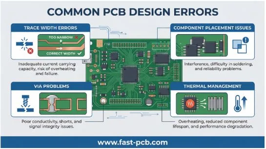
PCB traces act as the wiring of your circuit, carrying electrical signals between components. The geometry of these traces, specifically their width and thickness, is a critical design parameter. A common mistake, especially for beginners, is to use a default trace width for all connections. This can lead to serious issues, particularly with traces carrying significant current.
The Problem: When a trace is too narrow for the current it carries, it can overheat, leading to a drop in voltage, and in severe cases, a burnt-out trace. This can cause intermittent failures or a complete circuit malfunction. Conversely, unnecessarily wide traces can take up valuable board space, making routing more difficult and increasing the overall size of the PCB.
How to Avoid It: The IPC-2221 standard provides guidelines for determining the appropriate trace width based on the current carrying capacity and the acceptable temperature rise. Online calculators based on this standard are readily available and should be used to size power-carrying traces correctly. It’s also important to consider the copper thickness (measured in ounces per square foot). Thicker copper allows for narrower traces to carry the same amount of current. For high-power applications, using 2oz or 3oz copper is a common practice.
2. Inadequate Component Placement and Layout
As electronic devices become smaller and more compact, the pressure to create dense PCB layouts increases. However, cramming components too close together without a proper layout strategy can lead to a host of manufacturing and performance issues.
The Problem: Improper component placement can result in assembly problems, such as components overlapping or being too close to the edge of the board. This can make soldering difficult or impossible, leading to rework and increased costs. From an electrical standpoint, poor placement can introduce noise and interference between components, especially in mixed-signal designs (analog and digital).
How to Avoid It: A well-thought-out component placement strategy is essential. Group related components together, such as placing all components of a specific sub-circuit in the same area. Keep analog and digital sections of the board separate to minimize interference. Pay close attention to the orientation of components to ensure a logical signal flow. Always adhere to the minimum clearance specifications provided by your manufacturer to avoid assembly issues.
3. Improper Decoupling Capacitor Placement
Decoupling capacitors are essential for providing a stable power supply to integrated circuits (ICs) by filtering out noise and voltage fluctuations. However, their effectiveness is highly dependent on their placement.
The Problem: If decoupling capacitors are placed too far from the IC’s power pins, their ability to filter high-frequency noise is significantly diminished. The inductance of the longer traces between the capacitor and the IC can render the capacitor ineffective, leading to unstable IC performance and potential malfunctions.
How to Avoid It: Decoupling capacitors must be placed as close as possible to the power and ground pins of the IC they are intended to support. The connection traces should be short and direct. The ideal placement is on the same side of the board as the IC, directly connected to the power and ground planes.
4. Landing Pattern and Footprint Errors
The landing pattern, or footprint, is the set of pads on the PCB where a component is soldered. An error in the footprint dimensions can make it impossible to mount the component correctly.
The Problem: If the pad-to-pad spacing is incorrect, or the pads themselves are the wrong size, the component’s pins will not align properly with the pads. This can lead to soldering defects such as solder bridges (shorts between pads) or open circuits. These errors often necessitate a complete redesign and fabrication of the PCB, which is a costly and time-consuming process.
How to Avoid It: Always double-check and triple-check the component datasheets for the correct footprint dimensions. Most PCB design software includes extensive libraries of component footprints. Whenever possible, use these pre-verified footprints. If you need to create a custom footprint, be meticulous in following the datasheet’s recommendations. The IPC-7351B standard provides a comprehensive guide for surface mount design and land pattern standards.
5. Via Mismanagement
Vias are plated holes in a PCB that connect traces on different layers. While they are essential for routing complex boards, their misuse can introduce problems and increase costs.
The Problem: Overusing vias, or using advanced via types like blind and buried vias unnecessarily, can significantly increase the manufacturing cost of the PCB. From an electrical perspective, vias can introduce inductance and capacitance, which can degrade signal integrity, especially in high-speed designs.
How to Avoid It: Use vias judiciously. Plan your routing to minimize the number of layer changes. For most standard designs, through-hole vias (which go through all layers of the board) are sufficient and the most cost-effective option. Blind and buried vias, which connect an outer layer to an inner layer or two inner layers, respectively, should only be used when absolutely necessary for high-density designs, and their cost implications should be carefully considered.
6. Poor Thermal Management
Electronic components generate heat, and if that heat is not effectively dissipated, it can lead to component failure and a reduced product lifespan.
The Problem: Inadequate thermal management can cause components to overheat, leading to performance degradation and, eventually, permanent damage. This is a particularly critical issue for high-power components like voltage regulators, power amplifiers, and processors.
How to Avoid It: A good thermal design starts with identifying the heat-generating components on your board. Use large copper planes (pours) connected to the thermal pads of these components to act as heatsinks. Thermal vias can be used to transfer heat from the component to the inner or bottom layers of the PCB, where it can be further dissipated. For components that generate a significant amount of heat, a dedicated heatsink may be necessary.
7. Incomplete or Inaccurate Design Documentation
The final step in the PCB design process is to generate the manufacturing files, which typically include Gerber files (for the copper layers, solder mask, and silkscreen) and a Bill of Materials (BOM).
The Problem: Incomplete or inaccurate manufacturing files can lead to a host of problems, from incorrect component procurement to a completely non-functional board. Common errors include missing layers in the Gerber files, incorrect part numbers in the BOM, and ambiguous assembly instructions.
How to Avoid It: Before sending your design for manufacturing, perform a thorough review of all your design files. Use a Gerber viewer to inspect each layer and ensure that everything is correct. Meticulously check your BOM against your schematic to ensure that all part numbers, quantities, and descriptions are accurate. Providing clear and comprehensive assembly notes can also help to prevent misunderstandings during the manufacturing process.
Conclusion
PCB design is a complex process that requires a keen eye for detail and a thorough understanding of both electrical and manufacturing principles. By being aware of the common pitfalls and implementing the best practices outlined in this article, you can significantly increase your chances of a successful design. A little extra time spent in the design phase can save you a great deal of time, money, and frustration down the line. For a reliable and high-quality manufacturing partner, consider working with an experienced PCB provider like FASTPCB ONLINE QUOTE to bring your designs to life.