
Best Practices for Designing PCB Vias in Altium Designer
Printed circuit boards, or PCBs, are everywhere, from game consoles to medical devices. They’re like the streets of a busy city, connecting signals between different stops (or components). But sometimes, these streets need to go up or down levels, not just across the surface. That’s where vias come in. If you’re working in Altium Designer or with any custom PCB manufacturer, understanding vias will help you make better boards that work and last.
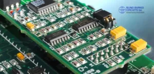
What Is a PCB Via?
Think of a via as a tiny tunnel. It allows electrical signals to travel from one layer of the board to another. Without vias, a PCB would be flat, with all parts fighting for the same limited space. Vias open up new paths below the surface, making compact, multi-layer projects possible.
There are several types of vias, but they all share a standard function: connecting different layers of a circuit. In Altium PCB design, you get complete control over how and where these vias are placed.
Types of PCB Vias
Through-hole via: the most common type. This hole goes from the top of the board all the way down to the bottom. It’s used when you need to connect everything, like a staircase that connects every floor.
- Blind via: This one connects the outer layer to an inner layer, but stops short of going all the way through. It’s suitable for saving space on crowded boards.
- Buried via: it’s completely sandwiched between inner layers. You’ll never see it from the outside. These are used in very dense boards, sometimes by advanced flex circuit board manufacturers.
- Microvia: much smaller than the others. Microvias are used in high-density boards, such as smartphones and tablets, where space is extra tight.
Why Vias Matter for Circuit Board PCB Design
As electronics become smaller and more complex, the need for layered connections increases. Vias help designers build boards that combine multiple circuits without occupying extra space. Without vias, you’d need huge boards, or lots of messy wires, to get the same function.
In practical terms, this means:
- Reduced board size, making electronics portable.
- Greater reliability, since shorter connections cause fewer signal problems.
- Lower costs for manufacturing, resulting from reduced waste of space and materials.
The Role of Altium Designer
Altium Designer is one of the most popular tools for circuit board PCB design. It gives you a layout where you can add and adjust vias exactly where you need them. Whether you work directly with a PCB manufacturer or a flex circuit board manufacturer, Altium’s software helps you meet their requirements.
You start by drawing the shape and layers of your board, then add components such as chips, sensors, and connectors. Vias are placed in spots where signals need to jump from one layer to another. Altium PCB design makes this step easier by letting you preview, adjust, and test via placement before you ever build a board.
Best Practices for Using Vias in Altium PCB Layout
Plan Layer Connections Early
Before dropping parts on your board, sketch a rough plan of how signals will move between layers. Try to keep paths short. Vias are helpful, but too many can create problems. Think of them like stairways, easy to use, but too many in one spot create a traffic jam.
Choose the Right Via Type for Your Needs
Don’t use a buried or blind via unless necessary. Through-hole vias work well in most designs and are easier (and less expensive) for your PCB manufacturer to produce. Reserve blind or buried vias for tight spaces or special signal paths.
Watch Via Size and Spacing
Every PCB manufacturer and flex circuit board manufacturer has guidelines for via sizes. Too small, and they might not be able to make them. Too big, and you waste space or risk crowding other parts. Check your manufacturer’s rules before starting your Altium PCB layout.
A good rule of thumb is to keep vias as small as safely possible, but leave enough room for reliable connections.
Group Vias for Power and Ground Connections
To help deliver stable power or create effective shielding from unwanted signals, place rows of vias (sometimes referred to as via fences) between specific layers. This strengthens the circuit and blocks interference.
Avoid Placing Vias Under Important Components
Vias under chips or connectors can weaken the solder joints or the board itself. If you must place a via near a component, double-check your design rules in Altium and obtain your manufacturer’s feedback.
Limit Number of Vias on Bend Areas in Flex PCBs
For flexible circuits, ask your flex circuit board manufacturer for advice. Bending the board can break vias placed right on the fold lines. Keep vias away from these areas to prevent cracking.
Test Your Design with Altium’s Tools
Altium Designer’s built-in checks catch many mistakes. Use the Design Rule Check (DRC) tool to identify vias that are too close, too large, or in the incorrect location. Fixing these issues in software saves time and money in the long run.
What Not To Do With Vias
- Don’t put vias too close together. This can make your board hard to build or cause short circuits.
- Don’t rely only on one manufacturer’s default settings. Request their latest information via the guidelines. Different companies employ different processes, particularly for specialized boards.
- Don’t ignore signal direction. Long, winding routes with numerous viaducts slow down signals.
- Don’t skip the preview step in Altium PCB design. Always review your layout and adjust via placement.
Working with Manufacturers
Bringing your design to life means sharing files with a custom PCB manufacturer or flex circuit board manufacturers. Here’s how to make that step smoother:
- Provide detailed Gerber files and Altium project files. These show exactly where your vias are, their size, and which layers they connect.
- Include documentation, especially for special via types (buried, blind, or microvia).
- Ask your PCB manufacturer or flex circuit board manufacturers for their latest capability charts. Determine their limits for via size, hole plating, and spacing before finalizing your design.
If you work together, you’ll get a board that matches your plan and stands up to use.
Common Questions
What are the most common mistakes for new designers?
Placing too many vias too close together, making them too small, or failing to follow the manufacturer’s guidelines.
How do I choose by type?
Through-hole for basic needs, blind or buried if space is a concern. Microvias are for ultra-dense, high-end boards.
Can I overuse vias?
Yes. More isn’t always better. Plan, only use what you need, and test your signal paths in Altium.
Does it matter who makes my PCB?
Yes. Not all manufacturers can accommodate every type of via or size, especially for advanced designs. Ask questions early.
Final Words
Creating great printed circuit boards requires paying attention to even the most minor details, including vias. The way you set up, place, and size your vias in Altium PCB design affects not only how well your board works, but also how long it lasts and even how much it costs. Start with a clear plan, utilize best practices, and always verify with your custom PCB manufacturer or flex circuit board manufacturer, like Blind Buried Circuits, before sending out your final files. Good design and teamwork will help bring your best ideas to life, one reliable connection at a time.