
How Electronic Devices Are Made: The Journey from Design to Your Hands
Every day, we interact with dozens of electronic devices without giving much thought to how they came to exist. Your smartphone alarm wakes you, your smart thermostat adjusts the temperature, your laptop powers your workday, and your fitness tracker monitors your evening run. These sophisticated gadgets feel almost magical in their capabilities, yet behind each one lies a fascinating manufacturing journey that transforms raw materials and innovative ideas into the technology that shapes modern life.
Understanding how electronic devices are made reveals not just an industrial process, but a complex orchestration of engineering expertise, precision manufacturing, rigorous testing, and global supply chains. Whether you’re a student considering a career in engineering, a consumer curious about the products you use every day, or a business professional exploring manufacturing options, this guide demystifies the remarkable process that brings electronic devices to life.
It All Starts with an Idea: Design and Development
Every electronic device begins as an idea—someone identifying a problem that technology could solve or envisioning a product that could improve people’s lives. Perhaps it’s engineers at a medical technology company conceptualizing a more accurate patient monitoring device, or a startup team imagining a more innovative way to manage home energy consumption. This initial spark sets in motion a development process that will ultimately result in a physical product.
The first stage involves detailed product design, where industrial designers sketch the device’s appearance and user interface, while electrical engineers design the internal circuitry that powers it. This phase requires balancing multiple considerations: the device must perform its intended function reliably, fit within size and weight constraints, meet safety and regulatory requirements, achieve a target manufacturing cost, and appeal to consumers aesthetically.
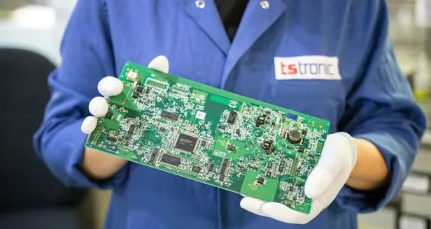
Modern electronic design relies heavily on sophisticated computer-aided design software. Engineers create virtual prototypes to simulate how circuits will behave before building physical versions. They design printed circuit boards—the green boards packed with components that form the heart of most electronics—carefully positioning hundreds or thousands of components and routing the copper traces that will connect them electrically. This digital design phase can take months or even years for complex products, with countless iterations refining performance, reducing costs, and improving manufacturability.
Once the design team is satisfied with their virtual prototype, they move to creating physical prototypes. These initial units, often hand-built in small quantities, allow engineers to verify that their designs work in the real world. Prototypes undergo extensive testing: Does the device perform as intended? Does the battery last long enough? Will it withstand being dropped? Does it overheat during extended use? This iterative process of building, testing, identifying problems, redesigning, and testing again continues until the team is confident they have a product ready for manufacturing.
From Prototype to Production: Preparing for Manufacturing
Having a working prototype is one thing; manufacturing thousands or millions of identical units reliably and affordably is quite another challenge. This transition from prototype to production represents a critical phase where many promising products falter. It requires expertise not just in product design but in manufacturing processes, supply chain management, and quality control.
Most companies choose to partner with specialized manufacturers rather than building their own factories. Electronic assembly has become a highly specialized field, with dedicated companies investing in the expensive equipment and expertise required for modern electronics manufacturing. These Electronics Manufacturing Services providers, as they’re known, handle the complex task of transforming designs into finished products.
Before full-scale production begins, manufacturers conduct what’s called New Product Introduction, a structured process that bridges the gap between prototype and mass production. Engineers from the product company and the manufacturing partner work together to optimize the design for efficient manufacturing. They suggest moving a component slightly to simplify automated assembly, swapping one part for an equivalent that’s more readily available, or adjusting a circuit board dimension to fit standard manufacturing equipment.
During this phase, manufacturers also develop all the documentation, programming, and tooling needed for production. Automated assembly machines must be programmed with precise coordinates for placing each component. Custom fixtures for testing must be designed and built. Quality control procedures must be established. Suppliers for all the necessary elements—which might number in the hundreds for a complex device—must be identified and qualified. This preparation is painstaking but essential; thorough groundwork during New Product Introduction prevents costly problems during volume production.
The Manufacturing Process: Building Electronic Devices at Scale
Once preparation is complete, actual manufacturing begins. For most modern electronic devices, the process centres on assembling printed circuit boards, those ubiquitous green boards that serve as both the structural foundation and electrical nervous system of electronics.
The process typically starts with bare circuit boards, manufactured separately at specialized facilities. These boards arrive with all the necessary copper traces and connection points already formed, but without any components attached. The first significant step is applying solder paste—a grey, paste-like substance containing tiny metal alloy balls—to specific locations on the board where components will be placed. This is done using a stencil printer, which works somewhat like screen printing a t-shirt, precisely depositing tiny dots of solder paste onto hundreds of designated spots.
Next comes component placement, accomplished by remarkable machines called pick-and-place systems. These automated marvels use cameras and precision robotics to pick up tiny electronic components from reels or trays and place them onto the circuit board with extraordinary accuracy. Modern pick-and-place machines can position components as small as a grain of sand with tolerances measured in thousandths of a millimetre, working at speeds that place tens of thousands of components per hour. Watching one operate is mesmerizing—the machine head darts across the board in a blur of motion, yet each component lands exactly where it should.
After all surface-mount components are placed, the boards travel through a reflow oven. This sophisticated piece of equipment gradually heats the boards to around 250 degrees Celsius in a carefully controlled temperature profile. As the temperature rises, the solder paste melts, creating permanent electrical and mechanical connections between components and the circuit board. The boards then cool slowly, leaving solid solder joints that reliably conduct electricity and hold components in place for years.
Some components—particularly larger ones like connectors or components subject to mechanical stress—use through-hole technology, where component leads insert through holes in the board. These are typically soldered using wave soldering, where the bottom of the board passes over a wave of molten solder, or selective soldering, where a precisely controlled solder fountain deposits solder at specific locations. Many modern devices use a combination of both surface-mount and through-hole technologies to optimize performance and reliability.
Quality Control: Ensuring Every Device Works Perfectly
Manufacturing components onto a board is only half the battle; ensuring every board is assembled correctly is equally critical. Modern electronics manufacturing uses multiple quality-control checkpoints to catch defects before they reach customers.
Immediately after solder paste application, sophisticated inspection systems examine each board to verify that the correct amount of paste was deposited in the proper locations. This Solder Paste Inspection catches printing problems before components are placed, preventing defects that would otherwise only appear later.
After component placement and soldering, Automated Optical Inspection systems use high-resolution cameras to photograph each assembled board from multiple angles. Sophisticated software compares these images with the expected appearance, identifying missing components, misplaced parts, solder bridges that create unwanted electrical connections, insufficient solder that might cause intermittent connections, and other potential defects. Some systems use 3D imaging to measure solder joint quality precisely, detecting subtle issues invisible to 2D inspection.
For components like microprocessors, where solder joints are hidden beneath the package, X-ray inspection reveals what optical systems cannot see, ensuring critical connections are correctly formed.
Beyond visual inspection, assembled boards undergo electrical testing. In-Circuit Testing uses a bed of spring-loaded probes to make contact with test points on the board, verifying electrical connectivity and component values. Functional testing goes further, powering up the board and running it through operational sequences to confirm it performs as designed. For a smart thermostat, this might involve cycling through temperature settings and verifying wireless communication. For a fitness tracker, this might include testing the sensors, the display, and the battery charging.
These multiple inspection layers work together to achieve remarkably low defect rates. Leading manufacturers, particularly those recognized as the best EMS company in Europe, routinely achieve defect rates below 100 parts per million—meaning fewer than one in ten thousand boards have any defects. This level of quality is essential for building reliable products that meet customer expectations.
Final Assembly: From Circuit Boards to Finished Products
For many devices, populated circuit boards are only one component of the finished product. Final assembly, often called box build in manufacturing terminology, transforms circuit boards into complete devices ready for consumers.
This stage varies enormously depending on the product. A simple device requires installing the circuit board into a plastic enclosure and adding a battery. A complex industrial control system might involve mounting multiple circuit boards, connecting cable harnesses, installing displays and controls, loading firmware, and performing extensive system-level testing.
Final assembly often occurs in climate-controlled environments, particularly for sensitive products such as medical devices and precision instruments. Workers follow detailed assembly procedures, usually supported by visual work instructions or even augmented reality systems that guide them through complex assembly sequences. Many manufacturers implement lean manufacturing principles, organizing workstations to minimize wasted motion and ensure efficient flow.
Once assembled, the devices undergo final testing to validate overall system performance. This might include running the device through its complete operational sequence, testing wireless connectivity, verifying battery life, checking display quality, and validating that all buttons and interfaces function correctly. Some products undergo environmental stress testing, operating them at temperature extremes or subjecting them to vibration to ensure reliability under real-world conditions.
Packaging, Logistics, and Distribution
After passing final inspection, devices move to the packaging area. This seemingly simple step actually requires considerable thought—packaging must protect the product during shipping, present it attractively to customers, include all necessary documentation and accessories, meet regulatory labelling requirements, and increasingly, minimize environmental impact through sustainable materials and efficient design.
Modern manufacturing often integrates directly with logistics systems, enabling manufacturers to ship products directly to retailers or even to individual customers, bypassing traditional warehousing. This approach, called direct fulfilment, reduces handling and speeds up product delivery to market. For companies selling globally, manufacturers might customize packaging to include different languages or regulatory markings for other markets, or even configure devices with region-specific software before shipping.
The Global Supply Chain: A Hidden Complexity
Behind this manufacturing process lies an extraordinarily complex global supply chain. A typical electronic device might contain components from dozens of suppliers across multiple continents. Microprocessors from Taiwan, displays from South Korea, sensors from Japan, passive components from China, connectors from Europe—all must arrive at the manufacturing facility at precisely the right time.
Managing this supply chain represents one of the most challenging aspects of electronics manufacturing. Component lead times can range from days to months. Unexpected shortages can halt production. Quality issues with incoming components can cascade through the manufacturing process. Professional manufacturers invest heavily in supply chain management systems, supplier relationships, and inventory strategies to navigate these challenges.
Recent years have highlighted supply chain vulnerabilities, with semiconductor shortages, shipping disruptions, and geopolitical tensions impacting electronics production globally. This has driven increased interest in nearshoring—producing goods closer to their ultimate markets—and supply chain diversification to reduce risk.
Innovation and Evolution: How Manufacturing Continues to Advance
Electronics manufacturing continues evolving rapidly, driven by advancing technology and changing market demands. Industry 4.0 concepts are transforming factories, with connected equipment providing real-time production data, artificial intelligence predicting quality issues before they occur, and digital twins allowing virtual optimization of production processes before implementing changes on actual production lines.
Miniaturization continues relentlessly, with components shrinking and circuit boards becoming more densely packed. This drives ongoing investment in more precise equipment and more sophisticated inspection systems. Simultaneously, the push toward sustainable manufacturing is driving innovations in energy efficiency, material recycling, and reduced waste.
Conclusion: The Remarkable Journey from Idea to Device
The next time you pick up your smartphone, activate a smart home device, or rely on any electronic device, you’re holding the culmination of an extraordinary manufacturing journey. From initial concept through detailed design, prototype development, manufacturing preparation, precision assembly, rigorous testing, and global logistics, creating electronic devices requires orchestrating countless processes, technologies, and people.
What appears simple on the outside—a sleek device that just works—embodies remarkable complexity within. Understanding this process gives us appreciation not just for the products themselves, but for the engineering ingenuity, manufacturing expertise, and global coordination that make modern technology possible. Whether these devices connect us to loved ones, monitor our health, power our businesses, or simply entertain us, they represent one of humanity’s most impressive manufacturing achievements—and the process continues advancing, promising even more remarkable devices in the years ahead.