
TFLN Foundry vs IDM: How to Choose a Manufacturing Partner for Your PIC Project
Choosing between a thin-film lithium niobate (TFLN) foundry and an integrated device manufacturer (IDM) is ultimately a question of responsibility. Each model must carry a PIC’s design intent through wafer fabrication, testing, photonic integrated circuit packaging, and scale-up, but it assigns control and handoffs differently. If those boundaries are unclear at the start, a strong layout can still miss its target in the finished device.
This guide helps PIC designers, equipment manufacturers, and OEM/ODM teams match project control, customization, and production needs to the right TFLN foundry or IDM model.
TFLN Foundry, Fabless, and IDM Models Explained
The semiconductor value chain has three core stages: design, wafer fabrication and assembly, testing and packaging.[1] Companies may combine these roles or vary their degree of vertical integration by product. A useful foundry vs IDM comparison therefore starts with the work that the provider actually controls.
| Model or role | Design control | Wafer fabrication | Packaging, testing, and final delivery |
|---|---|---|---|
| Foundry | The customer normally owns the layout and works within the supported process rules. | The foundry manufactures the wafer. | Packaging and testing may remain with the customer or another supplier. |
| Fabless workflow | The fabless company owns the product concept, design, and usually the related IP. | Manufacturing is outsourced to a foundry. | Back-end work is coordinated with an outsourced assembly, test, or packaging provider. |
| IDM | The IDM develops the product and controls the core design. | Wafer fabrication is handled within the integrated organization. | Testing, packaging, and final delivery are managed within the same organization. |
| Fab-lite | The company keeps selected design and manufacturing capabilities in-house. | Some products or process stages are outsourced. | Back-end work may be internal for one product and outsourced for another. |
These categories overlap in practice. An IDM may outsource a process step, while a foundry may add design support, wafer-level testing, or packaging. Two TFLN photonic chip foundry providers can therefore use the same label but deliver at different handoff points. Buyers should confirm the actual service boundary before comparing proposals.
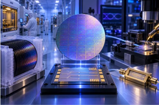
TFLN wafer for PIC fabrication
When a TFLN Foundry Is the Better Fit
A thin-film lithium niobate foundry is a strong fit when the customer has an experienced PIC design team, and the required circuit can be built with a standardized process. This model gives the customer direct layout control while using an established fabrication platform.
Projects are particularly well suited when they have the following characteristics:
- The design uses process design kit (PDK) rules and supported component libraries.
- Waveguides, electrodes, couplers, and other building blocks fit the available process modules.
- The customer can complete layout, simulation, design-rule checks, and tape-out preparation.
- Early prototypes can use a scheduled multi-project wafer (MPW) run.
A PDK connects the design environment to a specific manufacturing process through layer definitions, layout rules, component models, and verification files. In established PIC foundry programs, MPW runs place designs from several customers on one wafer. Sharing the run lowers the cost barrier for early prototypes and avoids an immediate commitment to a dedicated wafer.[2]
Standardization also sets boundaries. A shared run follows fixed materials, layer stacks, design rules, and schedules. A highly customized electrode, nonstandard waveguide, unusual material integration, or application-specific package may not fit without a dedicated process.
Before selecting TFLN foundry services, buyers should verify:
- PDK coverage: Are the required wavelengths, components, electrodes, and verification tools supported?
- Testing access: Which optical, DC, and RF measurements are available at wafer or die level?
- Packaging interfaces: Are fiber coupling structures, RF pads, dicing streets, and assembly requirements defined before tape-out?
- IP ownership: Who owns the customer layout, modified building blocks, process-specific improvements, and test data?
- Production path: Can the design move from MPW prototypes to a dedicated wafer run and repeat production without a major redesign?
The foundry model works best when its process boundaries match the design team’s intended level of control.
When a TFLN IDM Partner Is the Better Fit
Custom modulators and application-specific PICs often require decisions that cross the boundaries between design, fabrication, and packaging. An IDM partner can reduce these handoffs and keep technical feedback close to the engineers who can change the design or process.
- Design and process co-optimization. TFLN performance depends on material quality, nanofabrication, waveguide geometry, RF electrode design, and fabrication tolerances. A change in one area can shift optical loss, modulation efficiency, or bandwidth, so the chip and process must evolve together.[3]
- Chip and package co-design. Photonic integrated circuit packaging must preserve fiber coupling and electrical bandwidth while meeting the module’s footprint, thermal, and interface requirements. Package constraints can therefore influence the pad layout, coupling structure, and device architecture before tape-out.
- Short feedback loops and unified accountability. When design, wafer processing, testing, and packaging share one workflow, teams can trace a performance shortfall across the entire device. The team that identifies the problem can also carry the required change back into the design or process.
These advantages become practical when the partner connects the relevant engineering teams and facilities. Liobate’s TFLN technology platform links PIC design and wafer fabrication with high-density integration and packaging. For a nonstandard modulator, multi-channel circuit, specialized RF interface, or hybrid assembly, chip and package decisions can be made against the finished-device requirements. Results from packaged devices can then guide design or process adjustments without splitting the investigation across unrelated suppliers. This continuity is the IDM model’s main value for performance-sensitive customization.
How to Evaluate a TFLN Manufacturing Partner
Base the final choice on evidence from the complete development path. The same evaluation areas apply to both an IDM and a TFLN foundry.
| Evaluation area | Questions to ask | Evidence to request |
|---|---|---|
| PDK maturity and design support | Does the platform support the required functions and customization? How are design changes controlled? | PDK scope, design rules, supported building blocks, simulation models, and revision history |
| IP ownership | Who owns the layout, custom cells, process modifications, and generated test data? | Contract terms, licensing limits, reuse rights, and confidentiality provisions |
| Fabrication | Which tolerances control optical and RF performance? How is variation monitored? | Process windows, metrology records, wafer maps, yield definitions, and lot-to-lot data |
| Packaging and qualification | Can the package maintain coupling, RF, thermal, and reliability targets? | Packaged-device results, test conditions, environmental data, sample size, and acceptance criteria |
| Scale-up and supply-chain planning | How does a prototype move to pilot and repeat production? What happens when materials or processes change? | Capacity plan, lead times, change-control process, critical-source strategy, and long-term support plan |
Clear specifications are essential, but specifications alone do not prove repeatability. Qualification data should identify the device configuration, test method, operating conditions, sample size, and pass criteria. Batch-consistency claims should likewise use agreed measurements and acceptance limits. For scale-up, the supplier should explain how it will manage design revisions, process freezes, yield learning, packaging capacity, and material changes.
As an IDM manufacturing partner, Liobate supports projects that need more than a standard wafer handoff. Its integrated TFLN development capabilities align with three parts of the evaluation framework:
- Integrated development scope. Liobate has established platforms for TFLN PIC design, fabrication, and packaging. Its chip and device production lines cover wafer-level development and packaged devices.
- Custom engineering. Established in 2020, Liobate has developed extensive experience in customized chip tape-outs and packaged-device design deliveries. These projects include multi-channel, custom-voltage, and high-reliability modulators.
- Packaging around device performance. Its packaging development focuses on repeatable fiber-chip coupling, high electrical bandwidth, and hybrid integration with active components.
Liobate TFLN device portfolio
For PIC teams that need this combination of customization and integration capabilities, Liobate can discuss design ownership, performance targets, packaging interfaces, qualification requirements, and production plans. Contact Liobate to define the required development boundary for a custom TFLN chip or packaged device.
Conclusion
The best answer to “TFLN foundry or IDM?” follows from the project boundary. A foundry suits a customer-controlled layout that fits a mature PDK, standardized process, and defined packaging interface. An IDM becomes more valuable when custom device geometry, packaging-sensitive performance, qualification, and scale-up must be coordinated along a single development path. Evaluating both models against these criteria gives the PIC team the control it needs and makes responsibility clear from prototype to repeat production.
References
- OECD. Mapping the Semiconductor Value Chain. OECD Science, Technology and Industry Policy Papers, No. 182, 2025.
- Fahrenkopf, N. M., et al. “The AIM Photonics MPW: A Highly Accessible Cutting Edge Technology for Rapid Prototyping of Photonic Integrated Circuits.” IEEE Journal of Selected Topics in Quantum Electronics, 25(5), 2019.
- Zhu, D., et al. “Integrated Photonics on Thin-Film Lithium Niobate.” Advances in Optics and Photonics, 13(2), 242–352, 2021.