When crafting a PCB, you’ll want to carefully assess various essential elements to achieve optimal functionality. Component placement, routing optimization, and considering signal integrity are just the tip of the iceberg.
However, there’s a crucial factor that often gets overlooked but can significantly impact the overall effectiveness of your design. Choosing a reputable company like OurPCB can ensure quality manufacturing processes and reliable assembly, ultimately contributing to the success of your PCB project. Stay tuned to discover this critical aspect that could make or break your PCB project.
Key Takeaways:
- Efficient component placement and signal optimization are crucial for functionality and minimized interference.
- Signal integrity and power distribution are vital for reliable performance and stable voltage levels.
- Thermal management is essential to prevent overheating and ensure optimal device performance.
- Manufacturing efficiency is improved by streamlining design, reducing costs, and adhering to DFM principles.
Component Placement
When designing a PCB, consider the optimal component placement to ensure efficient functionality. Strategic placement of components is crucial for a well-designed circuit board. By carefully arranging components such as resistors, capacitors, and integrated circuits, you can minimize signal interference, reduce trace lengths, and optimize thermal management.
Begin by organizing components based on their functions and connectivity requirements. Group related components together to streamline signal paths and minimize the risk of electromagnetic interference. Pay attention to the orientation of polarized components to prevent errors during assembly and ensure proper functionality.
Furthermore, consider the proximity of components that frequently communicate with each other. Placing these components closer can reduce signal degradation and improve overall circuit performance. Be mindful of high-speed signal paths and critical components that require special attention to minimize noise and ensure signal integrity.
Routing Optimization
To enhance the efficiency of your PCB design, prioritize routing optimization to ensure optimal signal integrity and performance. Routing optimization involves carefully planning the paths of electrical traces on the PCB to minimize signal interference, crosstalk, and impedance mismatches. When optimizing routing, consider the signal frequencies, trace lengths, and the relationship between different signal paths.
Start by organizing components logically on the PCB to reduce trace lengths and ensure signal paths are direct and efficient. Utilize different signal layers effectively, grouping related signals together and separating high-speed and low-speed signals to prevent interference. Implementing proper trace width and spacing based on signal requirements helps maintain signal integrity and prevent signal degradation.
Additionally, use curved traces instead of sharp angles to reduce reflections and signal distortion. Avoid routing high-speed signals near noisy components or high-power traces to minimize electromagnetic interference. By optimizing routing, you can enhance the overall performance of your PCB design and ensure reliable operation of your electronic device.
Signal Integrity
Enhance your PCB design by prioritizing signal integrity, a crucial aspect that ensures reliable performance of your electronic device. Signal integrity refers to the ability of signals to propagate without distortion or loss, crucial for maintaining the quality of communication within your circuit. To optimize signal integrity, consider factors like trace length matching, controlled impedance routing, and minimizing signal reflections.
When designing your PCB layout, pay attention to signal traces’ length and impedance. Keeping trace lengths matched helps prevent timing mismatches and signal skew issues. Controlled impedance routing ensures signals reach their destinations without degradation, especially for high-speed signals. Additionally, reducing signal reflections by using termination techniques like resistors or capacitors enhances signal quality.
Employing ground planes effectively is another strategy to maintain signal integrity. Ground planes act as a reference for signals, reducing noise and interference. Proper power distribution and decoupling capacitors also play a vital role in ensuring stable voltage levels and minimizing noise.
Prioritizing signal integrity in your PCB design leads to improved performance, reduced electromagnetic interference, and overall reliability of your electronic device.
Thermal Management
Effective thermal management is crucial in PCB design to prevent overheating and ensure optimal performance of your electronic device. To achieve this, consider the following key points:
- Heat Dissipation: Proper heat dissipation is essential to prevent components from reaching critical temperatures. Utilize thermal vias, heat sinks, and thermal pads to efficiently transfer heat away from sensitive components.
- Component Placement: Carefully position heat-generating components on the board to minimize heat concentration in specific areas. Distributing these components evenly across the PCB can help in maintaining a balanced temperature profile.
- Airflow Considerations: Incorporate adequate ventilation in your design to facilitate airflow around the components. Ensure that vents, fans, or other cooling mechanisms are strategically placed to promote efficient heat dissipation and prevent hot spots on the PCB.
Manufacturing Considerations
Consider streamlining your PCB design to optimize the manufacturing process for efficiency and cost-effectiveness. Simplifying the layout of your PCB can significantly reduce production time and costs. Minimize the number of components and utilize standard sizes to make sourcing easier and more economical. When selecting components, prioritize those that are readily available and have shorter lead times to avoid delays in manufacturing.
Furthermore, ensure that your design complies with the manufacturer’s capabilities. Check the manufacturer’s design guidelines and specifications to guarantee that your PCB layout aligns with their manufacturing processes. This can prevent potential issues during production and improve overall product quality.
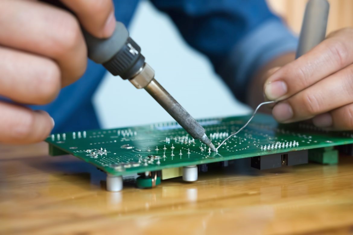
Incorporate Design for Manufacturing (DFM) principles into your PCB design to enhance manufacturability. DFM focuses on optimizing the design for efficient assembly, testing, and production. By following DFM guidelines, you can minimize errors, reduce rework, and accelerate the manufacturing process. Collaboration with the manufacturer early in the design phase can also help address any manufacturing concerns upfront, leading to a smoother production process.
How Does the Choice of PCB Material Impact the Performance of the Circuit?
When you choose a PCB material, it directly affects your circuit’s performance. Factors like dielectric constant, thermal conductivity, and cost influence how well your circuit functions. Select wisely to optimize your design’s efficiency.
What Are Some Common Mistakes to Avoid When Designing a PCB Layout?
When designing a PCB layout, avoid common mistakes like inadequate trace spacing, insufficient consideration for signal integrity, and overlooking thermal management. These errors can lead to performance issues and difficulties during the manufacturing process.
How Can Emi/Emc Considerations Impact the Design of a Pcb?
When designing a PCB, it’s crucial to consider EMI/EMC implications. Properly addressing these factors can prevent interference issues and ensure your PCB functions optimally. Implementing shielding, grounding techniques, and proper layout can mitigate these concerns effectively.
What Software Tools Are Commonly Used for PCB Design and Simulation?
When designing a PCB, consider factors like component placement, routing, and signal integrity. Use software tools like Altium Designer, Eagle, or KiCad for design and simulation. They offer features for efficient PCB development.
What Are Some Strategies for Reducing Cost Without Sacrificing Quality in PCB Manufacturing?
To reduce cost without sacrificing quality in PCB manufacturing, consider optimizing component placement, using standard materials, and minimizing board size. These strategies help streamline production processes and lower expenses while maintaining high-quality standards.