
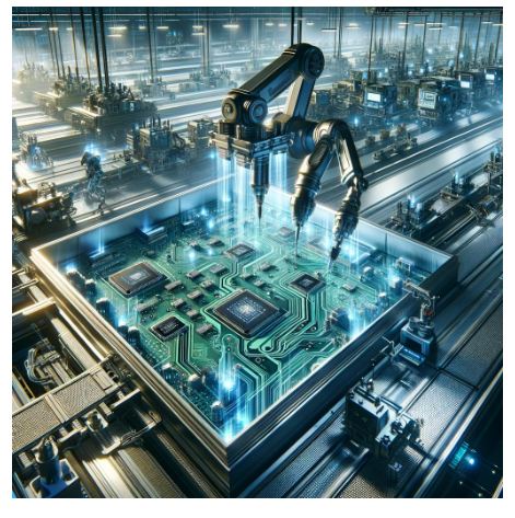
Efficiency in Action: Streamlining PCB Assembly with High Density Interconnect PCBs
As technology continues to advance, the demand for smaller, lighter, and more efficient electronic devices grows exponentially. High-Density Interconnect PCBs (HDI PCBs) have emerged as a key technology in achieving these objectives. In this article, we’ll explore how HDI PCBs streamline the assembly process, leading to increased efficiency and performance in electronic devices.
Introduction to High-Density Interconnect PCBs (HDI PCBs)
High-Density Interconnect PCB, or HDI PCBs, are specialized circuit boards designed to accommodate high-density component placement and intricate routing. Unlike traditional PCBs, which rely on through-hole vias, HDI PCBs utilize microvias and fine-line traces to achieve higher component density and signal integrity.
Understanding HDI PCBs
What are HDI PCBs?
HDI PCBs feature densely packed circuitry with multiple layers of copper interconnected by microvias. This allows for smaller and lighter PCB designs while maintaining or even improving performance.
Advantages of HDI PCBs
HDI PCBs offer several advantages over traditional PCBs:
- Increased Component Density: HDI PCBs allow for more components to be placed within a smaller footprint, enabling the creation of compact electronic devices.
- Enhanced Signal Integrity: Shorter interconnection lengths and reduced parasitic effects result in improved signal integrity and reduced electromagnetic interference (EMI).
- Reduced Weight: By eliminating the need for bulky through-hole components and connectors, HDI PCBs contribute to overall weight reduction in electronic devices.
- Improved Thermal Management: Compact designs enable more efficient heat dissipation, crucial for high-performance applications.
Applications of HDI PCBs
HDI PCBs find applications in various industries, including:
- Consumer Electronics: Smartphones, tablets, wearables, and other portable devices benefit from the compact size and high performance of HDI PCBs.
- Telecommunications: HDI PCBs are integral to the infrastructure of telecommunications equipment, enabling faster and more reliable communication.
- Medical Devices: Miniaturized medical devices rely on HDI PCBs for precise control and monitoring capabilities in constrained spaces.
Streamlining PCB Assembly with HDI PCBs
The unique features of HDI PCBs contribute to streamlining the PCB assembly process, resulting in increased efficiency and productivity.
Improved Component Density
HDI PCBs allow for higher component density, meaning more functionality can be packed into a smaller area. This results in fewer PCBs needed for a given project, reducing overall assembly time and cost.
Reduced Footprint and Weight
Due to their compact design, HDI PCBs contribute to smaller and lighter electronic devices. This not only enhances portability but also reduces shipping costs and environmental impact.
Enhanced Signal Integrity
The shorter interconnection lengths and controlled impedance characteristic of HDI PCBs contribute to enhanced signal integrity, reducing the risk of signal distortion or loss. This is crucial for high-speed and high-frequency applications where signal integrity is paramount.
Simplified Assembly Process
HDI PCBs simplify the assembly process by eliminating the need for through-hole components and connectors, reducing assembly time and labor costs. Additionally, the use of microvias allows for automated assembly techniques, further increasing efficiency and consistency.
Design Considerations for HDI PCB Assembly
While HDI PCBs offer numerous benefits, several design considerations must be taken into account to ensure successful assembly and optimal performance.
Component Placement and Routing
Careful consideration must be given to component placement and routing to minimize signal interference and ensure efficient assembly. Designers should optimize layout and utilize advanced routing techniques to maximize space utilization and signal integrity.
Thermal Management
Despite their compact size, HDI PCBs can generate significant heat, especially in high-performance applications. Proper thermal management techniques, such as heatsinks, thermal vias, and copper pours, are essential to prevent overheating and ensure reliable operation.
Manufacturing Constraints
Manufacturing HDI PCBs requires specialized equipment and processes, including laser drilling and sequential lamination. Designers must work closely with manufacturers to ensure that design specifications are compatible with manufacturing capabilities and constraints.
Case Studies: Real-world Examples of Efficient Assembly with HDI PCBs
Real-world case studies demonstrate the effectiveness of HDI PCBs in streamlining the assembly process and improving overall efficiency.
Future Trends in HDI PCB Assembly
As technology continues to evolve, we can expect ongoing advancements in HDI PCB assembly techniques and technologies. Future trends may include:
- Advanced Materials: Development of new substrate materials with enhanced properties to further improve performance and reliability.
- Miniaturization: Continued miniaturization of components and interconnects to achieve even higher component density and smaller form factors.
- Automation: Increasing automation in the assembly process to reduce labor costs and improve consistency and quality.
Conclusion
In conclusion, High-Density Interconnect PCBs (HDI PCBs) play a crucial role in streamlining the assembly process and increasing efficiency in electronic device manufacturing. By leveraging the unique features of HDI PCBs, designers can achieve higher component density, reduced footprint and weight, enhanced signal integrity, and simplified assembly processes. As technology continues to evolve, HDI PCBs will remain at the forefront of innovation, driving advancements in electronic design and manufacturing.