Sensor PCB: Design, Manufacturing, Benefits, and Applications
Sensors have become an essential part of modern electronic systems, enabling devices to detect, measure, and respond to changes in their environment. From automotive safety systems and industrial automation equipment to smart homes and medical devices, sensors provide the data needed for intelligent operation. At the heart of these sensing technologies is the Sensor PCB, a specialized printed circuit board designed to support sensor functionality, signal processing, and communication.
As the Internet of Things (IoT), artificial intelligence, and automation technologies continue to expand, the demand for high-performance sensor PCBs is growing rapidly. Understanding the design, manufacturing process, and applications of sensor PCBs can help businesses and engineers develop more reliable and efficient electronic products.
What Is a Sensor PCB?
A Sensor PCB is a printed circuit board specifically designed to integrate and support sensor components. These boards provide the electrical connections, power distribution, and signal processing pathways necessary for sensors to operate effectively.
Sensors detect physical, chemical, or environmental changes and convert them into electrical signals. The sensor PCB then processes, amplifies, filters, or transmits these signals to other electronic systems.
Depending on the application, sensor PCBs can support various sensor types, including temperature sensors, pressure sensors, humidity sensors, motion sensors, proximity sensors, gas sensors, optical sensors, and many others.
The design of a sensor PCB often focuses on accuracy, reliability, and signal integrity to ensure precise measurements and dependable performance.
Components of a Sensor PCB
A typical Sensor PCB consists of several important elements that work together to collect and process data.
The sensor itself is the primary component responsible for detecting environmental changes. Different sensor technologies are selected based on the application requirements.
Signal conditioning circuits are often included to amplify, filter, or convert sensor outputs into usable electrical signals. These circuits help improve measurement accuracy and reduce noise.
Microcontrollers or processors may be integrated into the PCB to analyze sensor data and execute programmed functions.
Communication modules such as Bluetooth, Wi-Fi, Zigbee, CAN bus, or Ethernet interfaces allow the sensor PCB to transmit data to external devices or control systems.
Power management circuits ensure stable operation by regulating voltage and protecting sensitive components from electrical disturbances.
Together, these elements create a complete sensing solution capable of monitoring and responding to environmental conditions.
Structure of a Sensor PCB
The structure of a Sensor PCB depends on the type of sensor and the intended application. However, most sensor PCBs share several common features.
The substrate material provides mechanical support and electrical insulation. FR4 is widely used due to its cost-effectiveness and reliability, while flexible materials such as polyimide may be used for wearable or compact devices.
Copper traces form the conductive pathways that connect the sensor, processing circuits, and communication interfaces.
Multilayer designs are common in advanced sensor PCBs, allowing for improved signal routing, noise reduction, and compact layouts.
Protective coatings such as conformal coatings may be applied to shield the PCB from moisture, dust, chemicals, and environmental contaminants.
The overall design must ensure stable sensor performance while protecting sensitive circuitry from interference.
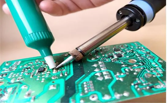
Manufacturing Process of Sensor PCBs
The production of a Sensor PCB follows a precise manufacturing process to ensure accuracy and reliability.
The process begins with PCB design and layout, where engineers optimize component placement and signal routing to minimize interference and maximize performance.
Copper-clad laminates are prepared, and the circuit pattern is transferred using photolithography techniques. Chemical etching removes unwanted copper, leaving the desired conductive traces.
Drilling and plating processes create vias and electrical connections between layers.
After fabrication, electronic components, including sensors and signal conditioning circuits, are assembled using surface-mount technology (SMT) or through-hole assembly methods.
Soldering, inspection, and testing are performed to verify electrical functionality and sensor performance.
In many applications, calibration is conducted to ensure accurate measurements before the final product is delivered.
Benefits of Sensor PCBs
One of the primary advantages of a Sensor PCB is its ability to provide accurate and reliable data collection. Proper PCB design helps reduce electrical noise and improve signal quality, leading to more precise sensor readings.
Another significant benefit is compact integration. Modern sensor PCBs combine sensing, processing, and communication functions within a single board, reducing system complexity.
Sensor PCBs also improve automation capabilities by enabling real-time monitoring and control of various processes.
Durability is another advantage. Properly designed sensor PCBs can operate in harsh environments, including high temperatures, humidity, vibration, and chemical exposure.
Scalability is also important, as sensor PCBs can be customized for a wide range of applications and industries.
These benefits make sensor PCBs a critical component in modern electronic systems.
Applications of Sensor PCBs
The versatility of Sensor PCB technology has led to its adoption across numerous industries.
In the automotive sector, sensor PCBs are used in tire pressure monitoring systems, engine management systems, parking assistance systems, airbag controls, and advanced driver-assistance systems (ADAS).
Industrial automation relies heavily on sensor PCBs for monitoring temperature, pressure, vibration, flow rates, and machine performance. These systems help improve efficiency and predictive maintenance capabilities.
Medical devices utilize sensor PCBs in patient monitoring systems, diagnostic equipment, wearable health devices, and imaging systems.
Consumer electronics incorporate sensor PCBs into smartphones, smartwatches, fitness trackers, smart home devices, and gaming systems.
Environmental monitoring systems use sensor PCBs to measure air quality, humidity, temperature, water quality, and pollution levels.
Agricultural applications also benefit from sensor PCBs, enabling precision farming through soil monitoring, weather tracking, and irrigation control.
Design Considerations for Sensor PCBs
Designing a Sensor PCB requires careful attention to several important factors.
Signal integrity is one of the most critical considerations. Sensor outputs are often low-level signals that can be affected by electrical noise. Proper grounding, shielding, and trace routing are essential for maintaining accuracy.
Power management must be optimized to ensure stable sensor operation, particularly in battery-powered devices.
Environmental conditions should be considered during material selection and protective coating design.
Thermal management is important for sensors that generate heat or operate in high-temperature environments.
Component placement should minimize interference while allowing efficient signal processing and communication.
Designers must also account for calibration requirements and manufacturing tolerances to ensure consistent performance across production batches.
Future Trends in Sensor PCB Technology
The future of Sensor PCB technology is closely linked to advancements in IoT, artificial intelligence, and smart devices.
Miniaturization continues to drive innovation, with manufacturers developing smaller and more powerful sensor PCBs for wearable technology and compact electronics.
Wireless connectivity is becoming increasingly important, allowing sensor systems to communicate seamlessly with cloud platforms and edge computing devices.
Flexible and rigid-flex sensor PCBs are gaining popularity in medical and wearable applications due to their ability to conform to complex shapes.
Artificial intelligence is also enhancing sensor systems by enabling real-time data analysis and predictive decision-making.
These trends are expected to further expand the role of sensor PCBs in next-generation electronic products.
Conclusion
The Sensor PCB plays a vital role in modern electronics by enabling accurate data collection, signal processing, and communication across a wide range of applications. From automotive systems and industrial automation to healthcare devices and smart consumer products, sensor PCBs provide the foundation for intelligent and responsive technologies.
As industries continue to embrace automation, connectivity, and real-time monitoring, the demand for advanced sensor PCB solutions will continue to grow. Companies seeking high-quality sensing solutions often work with an experienced Sensor PCB manufacturer to ensure reliable performance, precise measurements, and long-term product success.